 |
| OwenDuffy.net |
|
This article describes an application of PllLdr to an Si4133GT PLL, the VK3XDK Agile PLL V2.
|
|
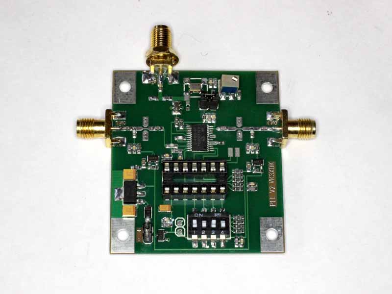
Fig 1 shows the target PLL board, a VK3XDK AgilePLL V2 (with Picaxe controller chip removed). The PICAXE chip on the AgilePLL has been removed and a DIP header plug used to connect a prototype PllLdr to the board. A wire has been connected from the AUXOUT pin (lower right) to pin 13 of the DIP socket (unused in the original). This connects the AUXOUT (used for LDETB) to the PllLdr.
Differently to the V1 board, this V2 board has a Si4133-G chip (which has programmable R divider), provision for optional MMICs in each output, and an optional 10MHz TCXO on board.
The board is supplied without a circuit diagram which is frustrating, time has been wasted.
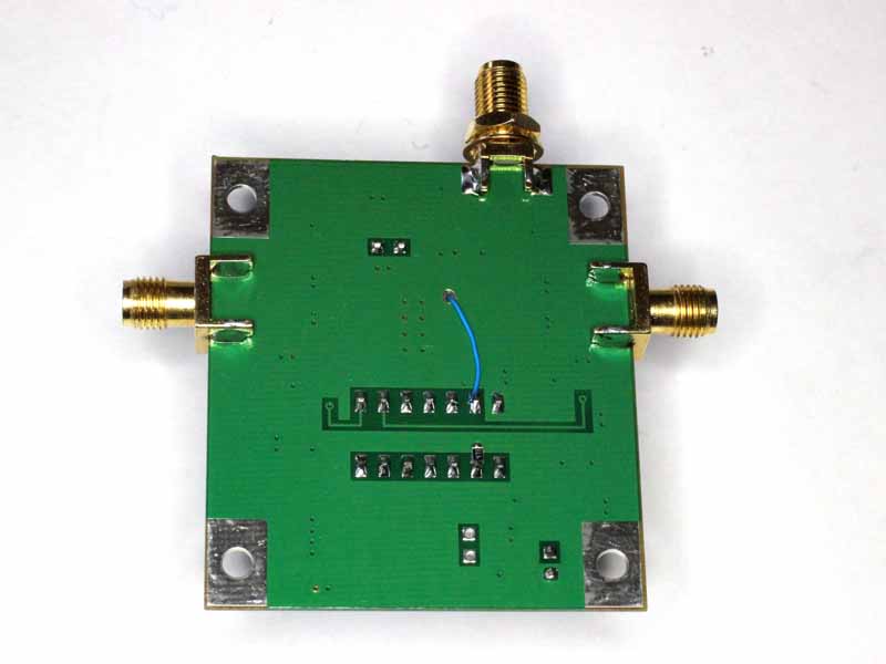 |
Fig 2 shows the link connecting AUXOUT to the DIP socket.
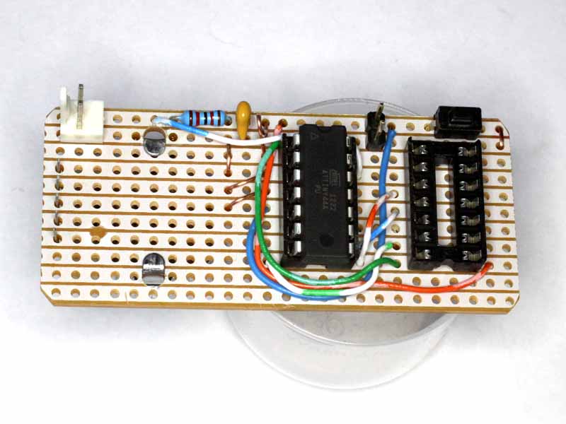 |
Fig 3 shows the prototype PllLdr module. The right hand socket is for the DIP cable to the PLL board.
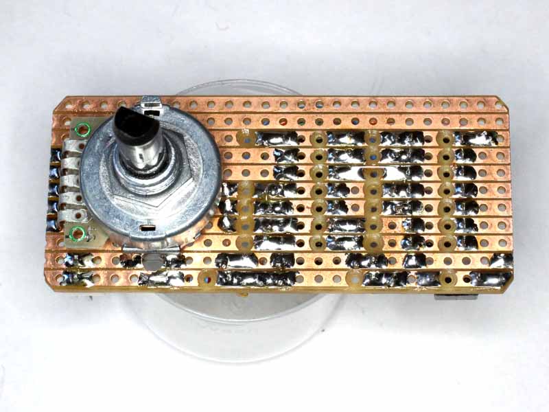 |
Fig 4 shows the underside of the PllLdr board.
The switch used is a 4 bit Gray coded switch, and the address offset feature of PllLdr is used to rotate the 0 position to 12 o'clock. The Gray code switch was chosen for these tests as one is sure that rotating the switch one position does not feed some intermediate binary code to the system.
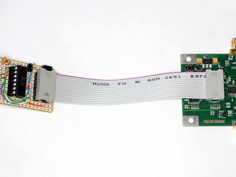 |
Fig 5 shows the DIP cable linking the PllLdr board to the PLL board.
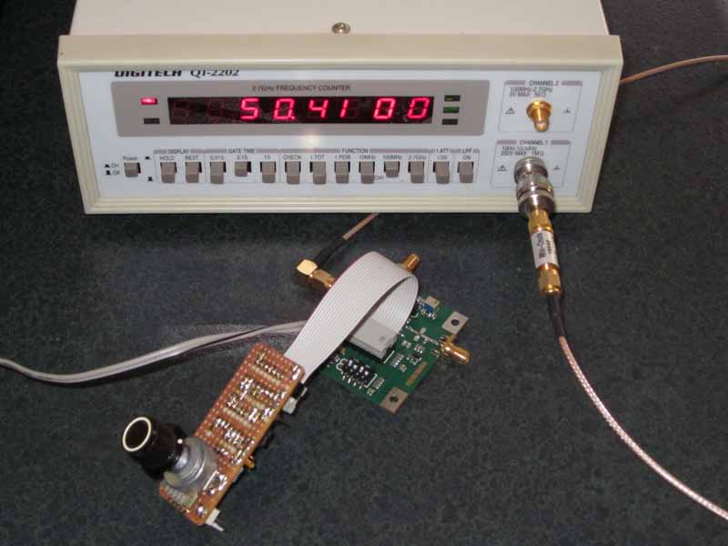 |
Fig 6 shows the combination under test.
The Si4133G has three PLLs, RF1 and RF2 share a single output port so only one can be used at a time, and another designated IF.
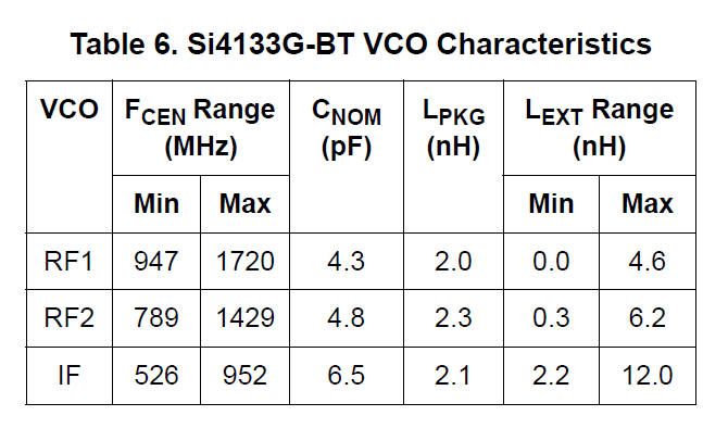 |
The stated range of centre frequencies (CF) supported are given in the datasheet as shown in Fig 7. The centre frequency is determined by the internal inductance and capacitance and the external inductor. This does not imply the VCO lock range.
When a device is built with a particular value of inductor, it has a certain range over which the VCO can be controlled, and that range is found by measurement as explained in AN31. This represents the range of frequencies that the VCO can lock at at the given temperature, voltage etc. The lock range with variation in temperature, voltage etc will be reduced somewhat.
The Si4133 datasheet describes the process:
Self-Tuning Algorithm
The self-tuning algorithm is initiated immediately after powerup of a PLL or, if the PLL is already powered, after a change in its programmed output frequency. This algorithm attempts to tune the VCO so that its freerunning frequency is near the desired output frequency. In doing so, the algorithm compensates for manufacturing tolerance errors in the value of the external inductance connected to the VCO. It also reduces the frequency error for which the PLL must correct to get the precise desired output frequency. The self-tuning algorithm will leave the VCO oscillating at a frequency in error by less than 1% of the required
output frequency.
After self-tuning, the PLL controls the VCO oscillation frequency. The PLL will complete frequency locking, eliminating any remaining frequency error. Thereafter, it will maintain frequency-lock and compensates for effects from temperature and supply voltage variations.
The Si4133G’s self-tuning algorithm compensates for component value errors at any temperature within the specified temperature range. However, the ability of the PLL to compensate for drift in component values that occur after self-tuning is limited. For external inductances with temperature coefficients approximately ±150 ppm/°C, the PLL can maintain lock for changes in temperature of approximately ±30°C.
Applications in which the PLL is regularly powered down (such as GSM) or switched between channels can minimize or eliminate the effects of temperature drift because the VCO is re-tuned when it is powered up or when a new frequency is programmed. Applications in which the ambient temperature can drift substantially after self-tuning, it might be necessary to monitor the LDETB (lock-detect bar) signal on the AUXOUT pin to determine the locking state of the PLL. See "Auxiliary Output (AUXOUT)" on page 18 for how to select LDETB.
So, after locking, the ability of the PLL to compensate for changes in VCO components with temperature etc is limited to about ±0.5%, but if the Self Tuning process is re-driven, the available lock range is much greater. The LDETB signal can provide the cue to the external circuit to re-drive the Self Tuning process.
Configuration data for the PllLdr is held entirely in EEPROM. In the following tests, different EEPROM images are created using an online generator at MCU to load PLL configuration registers. The EEPROM image when generated is downloaded to a workstation and loaded to the PllLdr AVR chip using the programmer shown in Fig 3.
The combination was tested for amplitude keying of the oscillator by turning the oscillator on and off using register 2.
|
#EEPROM data file for Si4133 |
Above, the PllLdr configuration for the keying test.
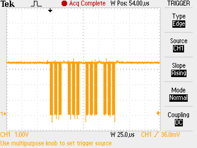 |
Fig 7 shows the PllLdr data transfer for writing four Si4133 registers, it takes just over 100µs which is sufficiently fast to allow keying of the PLL at Morse code speeds.
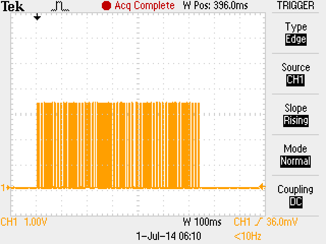 |
Fig 8 shows the original Picaxe data transfer, which at nearly 700ms is way too slow for practical Morse code keying speeds using this technique of selecting registers using the key input.
The keying was observed with a 50MHz CW receiver and keying was clean, T9 note. The test is recorded in a short video.
This test was to find the range of RF1 and RF2 VCOs using the procedure set out in AN31.
|
#EEPROM data file for Si4133 |
An EEPROM image with register settings for high and low frequencies for If, RF2 and RF1 was created.
The configuration was loaded and the range of each VCO observed at 20°:
The range is about ±15% about the geometric mean centre frequency (CF).
The AgilePLL was heated with a hair dryer and cooled with freeze spray, and the change in frequency noted. The variation in frequency was about ±6MHz at 1024MHz, or about ±0.6%. When that is allowed for, for reliability, the application should not use more than about ±13% of CF.
Nevertheless, SiLabs cautions against using more than ±5%:
Q: The PLL I am using has a tuning range larger than ±5%. Can I use this larger range in my application?
A: This is not recommended and should only be done after extensive experimentation. The ±5% tuning range
is designed to compensate for tuning inductor variations and provide sufficient margin for PCB manufacturing
process variations. Therefore, the tolerance of the tuning inductor should always be taken into account.
Ranges as large as ±12% have been observed during laboratory experiments. However, such large ranges
cannot be guaranteed due to concerns about changes in the operating conditions (temperature, supply
voltage, etc.) as well as the tolerance of the tuning inductor.
Where the tolerance of the inductor is eliminated by hand tuning, part of their allowance for inductor tolerance can be reallocated to operating range. They state that they have included ±10% allowance for inductor tolerance, which translates to ±5% of frequency, so it may be quite sound to add that ±5% inductor tolerance back into their ±5% composite range to achieve ±10% working range where the inductor is trimmed to the desired CF.
Applying that logic to this particular board:
Note that the CF can be changed by changing the relevant inductor. The RF1 and RF2 inductors are adjustable by moving the solder short, the IF inductor is a SM component which by calculation, appears to be 22nH.
The IF VCO range did not allow it to divide down to 144MHz, the required inductor would need to be around 10nH.
Temperature tolerance and the use of LDETB to maintain reliable lock is discussed in the context of the earlier version Agile PLL at PllLdr application - Si4133G (VK3XDK Agile PLL), and applies to this board. Tests were conducted for proper operation of LDETB monitoring and some firmware changes made to improve control stability.
The project was intended for experimentation rather than committed to a particular transverter use. The PLL was housed in a die cast box and all relevant controls and interfaces extended to the exterior.
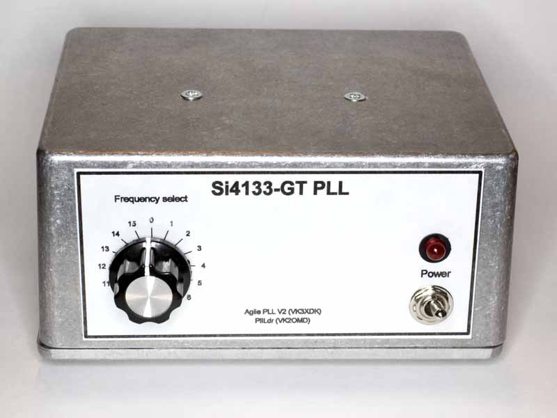 |
Fig 10 shows the front panel with 16 position frequency select switch and DC power switching / indication.
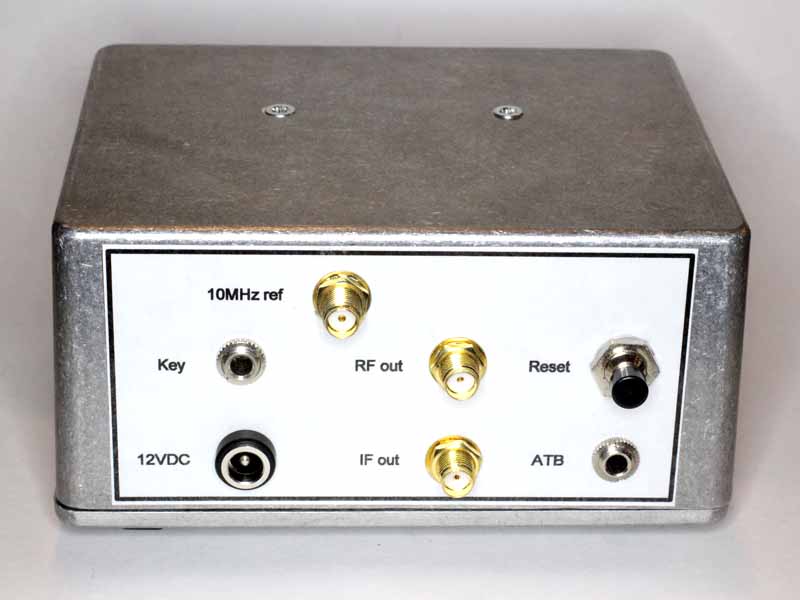 |
Fig 11 shows the rear panel. Sockets provide access to the reference input, PLL outputs, ATB programming interface, key and power.
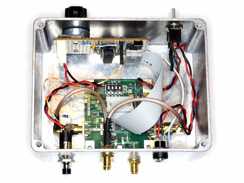 |
Fig 12 shows the interior cabling etc.
The ATB jack has since been rewired for Tx+Rx (using a diode) on R, and reset on T.
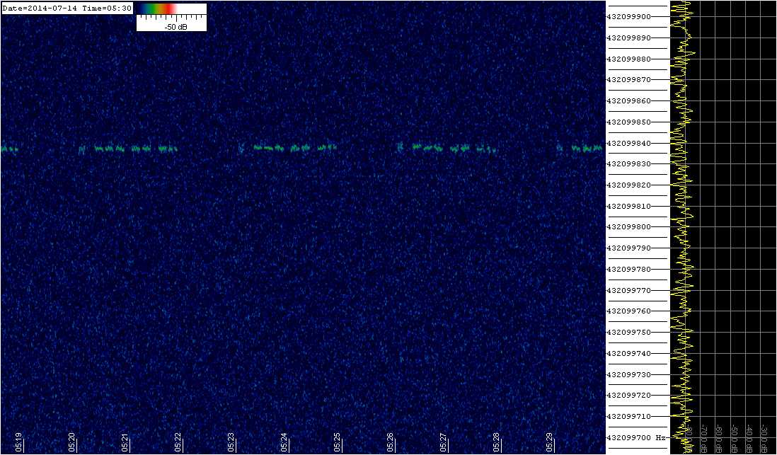 |
Fig 13 shows a grabber screen of the PLL modulated by a dual speed QRSS keyer (Another Morse beacon keyer - A/B RF switching).
In this case, the signal is 20dB below the noise in 2500Hz, it is not audible to the ear, and the partial call sign is quite distinguishable (OMD in QRSS3). The fuzzy trace at the beginning of each group is a 12WPM ID with the full callsign.
| Version | Date | Description |
| 1.01 | 01/07/2014 | Initial. |
| 1.02 | ||
| 1.03 | ||
| 1.04 | ||
| 1.05 |
© Copyright: Owen Duffy 1995, 2021. All rights reserved. Disclaimer.