 |
| OwenDuffy.net |
|
A kit from QRP Labs / Hans Summers finally arrived after 25 days (several other UK shipments arriving in 10 days during that time).
In sorting the parts, it is noted that with the exception of two caps in the output filter low grade caps (D>0.015) are used throughout. Lossy capacitors reduce power output at the fundamental, and more importantly, degrade harmonic suppression.
Better capacitors will be used in the output stage for this implementation, which necessitates review of the output network.
The device is intended to produce 100mW of RF output on 5V.
|
|
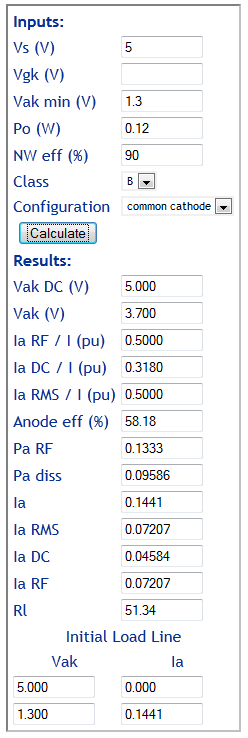
Fig 1 shows a calculation of an initial load line using Calculate initial load line of valve RF amplifier . Though this tool is design for valve PAs, it is quite applicable to the 2N7000 PA in this circuit. The resonant load impedance seen by the drain of the 2N7000 output FET needs to be about 50Ω.
The 9 pole output filter was supplied with two low loss ceramic 680pF caps, and two lossy 270pF caps. The network was redesigned to use 220pF caps on hand and the supplied good 680pF caps.
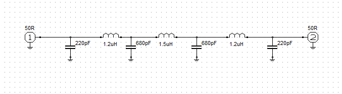 |
Fig 2 shows the revised circuit.
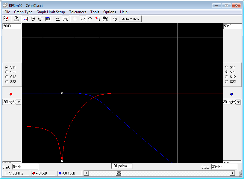 |
Fig 3 shows the response of the revised circuit.
Capacitor C11 is not only low grade, it has rather high reactance for the application and was replaced with a 0.01µF cap.
It is hard to understand why there are so many turns on L2. Excessive turns risks low self resonance and possibly lower impedance than intended.
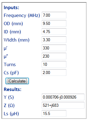 |
Fig 4 shows the redesigned choke L2 (using Calculate ferrite cored inductor). It has quite adequate impedance with just 10 turns.
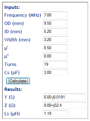 |
Fig 5 shows the design for L3 and L5, 19 turns give the closest match to the needed 1.2µH.
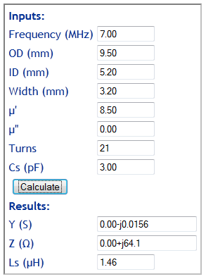 |
Fig 6 shows the design for L4, 21 turns give the closest match to the needed 1.5µH.
As it happens, the number of turns for L3, L4 and L5 are the same as those specified in the original circuit for the different capacitors.
The keyer chip was replaced with a Simple Morse beacon keyer for better flexibility, the chip is an ATTiny25. The relevant pins may yet be wired out to an external socket for convenient message text replacement.
To better facilitate 'stacking' 10min images from a grabber, a version of the Simple Morse beacon keyer to use a crystal oscillator for more accurate timing was developed and the board modified to add the crystal and related capacitors.
The circuit changes include:
Pinout for the modified keyer is different to the original keyer, and the chip is different. The code and data will not fit in an ATTiny13.
If you are buying a chip for this project, it may be wise to get a 20MHz ATTiny45 or ATTiny85, as future enhancements might require a larger chip. (ATTiny45 and ATTiny85 are about US$2 at Futurlec.com.)
The improved keyer used stores the message content and some options in EEPROM, no message content is compiled into the firmware. The message can be changed by replacing the EEPROM contents using a hex file created by the online tool at Simple Morse beacon keyer an inexpensive AVR programmer ($5) and free software (see the article for more information).
A small sub board was constructed to hold the AVR 6 pin ISP connector and mount it to the case for external access.
The kit runs on 5V and is limited by the maximum voltage that the keyer chip can withstand. There is no provision on board for a regulator from the common shack standard of 13V.
A low power MC34063 based DC-DC converter module purchased for a few dollars on eBay will be used to power the kit from 13V. The converter will allow operation from 5 to 30V, current drawn at 13V is 30mA.
The beacon was powered, and bias adjusted for a little over 100mW on 5V supply. The transmitter reconciles well with the model in Fig 1. Frequency was adjusted and the gimmick capacitor trimmed for 5Hz FSK.
About 20mA is drawn from the 5V supply with the PA cut off, and with the PA adjusted for 100mW,
current is almost 70mA. The instructions say Q3 should not get noticeably
warm
but in this instance, it is difficult to tell that it is any warmer
than any of the other transistors. Dissipation in the 2N7000 is around 100mW,
well within its ratings.
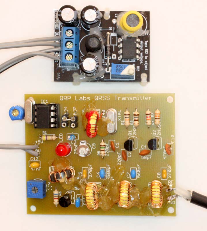 |
Fig 7 shows the constructed kit (as modified) under test. Inductors have been fixed in place with hot melt adhesive, and the turns on L1 lacquered to help oscillator stability. L1 was wound with thinner wire than supplied in the kit to avoid crowding and multi layer winding. The board layout uses unnecessarily small solder pads, the pad layout for the transistors is not the same as the packages, resistors were a tight fit, and some holes that beg the use of header pins are not of suitable spacing. It would be better to orient the toroids at 90° to each other as there is considerable flux leakage from low µ toroids such as these. The overlay does not match some of the component values for the 40m version.
The modification to use a crystal oscillator for the MCU clock can be seen, the crystal and its trimmer are at the top right of the picture, other required capacitors are under the board. The revised keyer allows more accurate timing to facilitate 'image stacking'.
The small module at the top of Fig 7 is a battery efficient DC-DC converter to power the transmitter from 6 to 30V.
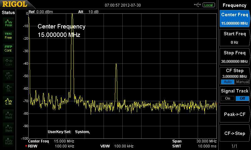 |
Fig 8 shows the transmitter output spectrum. There is a 20dB attenuator
between the transmitter and spectrum analyser. Indicated power is 0dBm at 7MHz,
so transmitter power is 20dBm or 100mW. The second harmonic is 40dB down which
complies with the Australian requirement for frequencies less than 30 MHz —
the lesser of: (i) 43 + 10 log (PEP) dB; and (ii) 50 dB
or 33dB for 100mW.
| Version | Date | Description |
| 1.01 | 15/06/12 | Initial. |
| 1.02 | ||
| 1.03 | ||
| 1.04 | ||
| 1.05 |
© Copyright: Owen Duffy 1995, 2021. All rights reserved. Disclaimer.