 |
| OwenDuffy.net |
|
This article describes the design and implementation of a simple semi automatic electronic Morse code keyer.
The keyer assists the formation of correctly times Morse signals by automating the timing of the duration of the dit and dah elements and the rest period between the dits and dahs, and optionally, between individual characters. The keyer also allows automatic generation of successive dits, successive dahs, and alternating dits and dahs or dahs and dits without keying each individual element.
Key design criteria were:
The functions that would be supported were:
Functions that would not be supported included:
This keyer will not suite grid block keying, any kind of valve cathode keying, any kind of high voltage keying without modification. It would be possible to use the keyer to key a suitable reed relay which in turn keyed one of these types of transmitter systems.
The implementation does not include a side tone oscillator, most (all) transceivers have a side tone function and it sounds better than a shabby implementation in a keyer, although I concede that a side tone oscillator in the keyer is handy for practice. You could add a small oscillator and speaker or phone jack yourself.
The right place to fix a bias problem if you have one is in the transmitter, not in the keyer, there shouldn't be a need for bias adjustment in the keyer.
Non standard Morse timing is not enhanced Morse, it is just a
barrier to effective communication. If you want to
"Swing", use a hand key. The PIK timing is compliant with
RECOMMENDATION ITU-R M.1677 International Morse code (2004).
I don't doubt that a repertory memory in a keyer may be handy, but nothing competes with a keyboard and screen if you want to have boilerplate stored and develop "macros", you have the power to implement an integrated decoder, and gee you could even create automated responses so you don't even need to be there!
One could approach the implementation a number of ways, including:
There is nothing novel about 1, it has been done before and there are so many designs in existence. The disadvantage is the number of chip packages and the amount of wiring favours a printed circuit board for implementation. This approach fails design criterion #1.
Implementation with a programmable logic array is relatively novel, but a gross overkill, expensive, and creates some construction difficulty with the package for the PLA. This approach fails design criterion #3.
An MCU implementation could again be an overkill, depending on the choice of MCU. The amount of software to implement a basic function set is quite small, the instruction path lengths are short, and only 3 or 4 I/O pins are required so a very modest MCU will be more than capable.
|
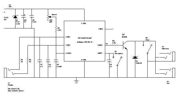
I have chosen a Microchip PIC12C508A, which is available in low cost plastic DIP8 package for through hole or socket mounting, has enough I/O pins, more than enough program memory and data memory, and plenty of CPU power for the job. The only downside of the 12C508A is that it is an OTP (one time programmable) which is one of the reasons why it is so cheap. An alternative would be a flash PIC chip like the 16F84, but since the software is so simple and should be stable, the added cost for the erase / reprogram capability is of little value once the development is done.
The design uses 1mA to 4mA at 5V, depending on speed and traffic. The zener regulator shown in the circuit will cause consumption of 10mA at 13.8V, it may be possible to reduce this by a few mA using a 78L05 regulator (although they can be a little hard to get). The VDD supply should not exceed 5V, but should run satisfactorily on 4.5V or 3V from series dry cells (although the speed range may change a little).
The chip provides two outputs, TX which goes to 5V for key down condition, and ~TX which is its inversion. These chip output pins are not open collector, do not short them to 0V for 5V (for example by putting a key or switch in parallel with the outputs). They are both provided for convenience for integration in a transmitter / transceiver.
The components are chosen to support a speed range of at least 10wpm to 40wpm. Based on a dit element duration of 120ms at 10wpm, the software is calibrated so that the oscillator runs at 10kHz. With the components shown, the prototype ranged from 6wpm to 50wpm (see Detailed derivation of Timing).
The schematic is shown in Figure 1. The circuit schematic is also available in Acrobat format here.
The MCU operates in the External RC Clock mode, clock frequency is set by VR1, R6 and C3. The clock runs at 10kHz for 10 wpm nominal speed, and should produce a dit element duration of 120 ms, or a repeating dit frequency of 4.2 Hz. Clock speed is sensitive to VDD, and range calibration will change if you try to run the chip at 2V. Clock speed is a compromise between timing granularity and risk of RFI. With the choice of 10kHz at 10wpm , the basic cycle time of the MCU is 0.4ms, which provides timing granularity of 0.4ms for a dit interval of 120ms, which is a granularity (timing resolution accuracy) of under 0.5%.
Timing of all elements (dits, dahs, rests and inter-character space) is derived from the single oscillator, is fixed requiring no alignment or adjustment, and is quite accurate.
This section applies to V1.13. The algorithm in V1.12 is identical apart from the sleep.
For the technically minded, the following is a brief description of the algorithm:
Main loop
Sending a dit or dah:
Executing autospace wait:
Sleeping:
Except for Iambic sequences, one must have the paddle closed at the time one wants an element to be initiated, and one must release the paddle anytime until the completion of the rest period to avoid sending another of that element type. This is true even when autospace forces an inter-character idle.
If while sending a dit (key down or rest period), one closes the dah paddle, a request for that dah be queued. One must release the dah paddle anytime until the completion of the rest period for the dah to avoid sending or queuing another dah. The converse also applies.
This is I believe referred to as Iambic Mode B operation, whereas Iambic Mode A would not queue the dah during the dit time, the dah paddle would have to be closed at the completion of the rest period following the dit to initiate the following dah. A Mode A keyer is short one of the features of a Mode B keyer. To my mind, an operator who exploits the capability of a Mode B keyer will notice the lack of iambic queuing in a Mode A keyer, whereas an operator accustomed to Mode A keyer will probably not notice any difference using a Mode B keyer.
If autospace is enabled, and neither paddle contact is closed at the completion of a rest period, the keyer will start a wait interval of a further two rest periods (during which it scans and latches the paddles), thereby forcing a standard inter character space.
I experimented with a range of schemes for the interval when the paddle latches were active, and when they were reset, monitoring error rates keying slow and fast, fresh and fatigued. This scheme above seemed most tolerant of my keying. On later checking, I think that the algorithm described above is identical to the operation of the once popular WB4VVF Accu-Keyer, though the timing is more accurate than the Accu-Keyer. Perhaps that is in part due to my training on an Accu-Keyer some twenty years ago!
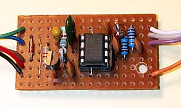 |
Fig 2 shows the prototype built on a piece of Veroboard 25mm x 42mm. The MCU is socketed so that the chip could be changed easily. All electronic components beside the pot are on the Veroboard, 15 parts in all 4 of which are for the regulated power supply.
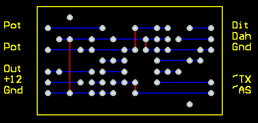 |
Figure 3 shows an example veroboard layout. The view is of the component side. The blue (horizontal) tracks are the veroboard tracks as used, the red tracks (vertical) are jumpers. Note that the tracks are cut between holes in some instances. Also note that the three jumpers are under the IC or its socket, they need to be installed first. This board layout does not include provision for mounting, you may need to provide additional space for the mounting system that you intend to apply, you could cut it overall to fit the slots of a jiffy box, or leave an extra 3 strips on one side and drill it to fit on threaded pillars. (Note that with subsequent revisions, the ~TX line is gone, and the ~AS pin is now AS). The Dit and Dah lines are actually ~Dit and ~DAH.
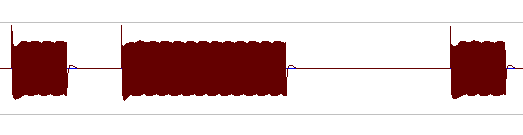 |
Figure 4 is a time domain display of a practice oscillator keyed by the PIK with the PIK oscillator running at 10kHz, sending the characters AE with Auto-space enabled.
The oscillator output was recorded digitally and the duration of the tone bursts and intervals were measured with resolution better than 1ms. The duration of the tone bursts and silent intervals are 120ms, 120ms, 360ms, 360ms and 120ms. The last dit was delayed by the Auto-space, the 360ms interval is a test of the Auto-space timing.
This keyer does not suffer any irregular timing of any elements as is evidenced in some other keyer designs, especially those that start the clock oscillator after an idle period and suffer irregular timing on the first cycle.
All significant timings and latencies are a function of the clock frequency which is adjusted for sending speed. The accuracy of the timing in relative terms should be equally good at all (practical) operating speeds. I looks just as good at 60wpm where the tone burst may be only 12 cycles of the side-tone oscillator.
The V1.14 MCU firmware licensed for individual non-commercial use can be downloaded here.
Switches, pot, jacks and a case will comprise most of the other costs, the whole thing should be less than A$30 for switches, pot, jacks, case, MCU, and the other parts.
Version 1.11 firmware was modified to reduce idle current consumption for battery operation. It did that in two ways, one is entering a sleep mode where the processor shuts down when idle (between characters sometimes), and changing the sense of the Autospace switch (switch open is Auto ON).
The sleep feature introduced in version 1.11 firmware has a problem that occurs rarely and is difficult to replicate, and has been removed from V1.12. All V1.11 chips were replaced and have been destroyed.
It turns out that the problem with V1.11 was with ringing of the paddle inputs at the instant that the MCU was entering sleep. The fix is to increase the values of C1 and C2 to 0.1uF.
Version 1.13 firmware reduces idle current consumption for battery operation. It achieves that by entering a sleep mode where the processor shuts down when idle (between characters if Autospace is off). Because the MCU reinitialises during normal operation, the ~TX line has been removed due to the very short glitch on that line during MCU initialisation.
When idle (sleeping) and Autospace ON, the prototype keyer (exclusive of the regulator) draws 1.5uA on a 5V supply, and when keying, current rises to 1.5mA. It is practical to run this version on 3 x AA alkaline cells (~3000mAh), battery life on idle would be limited by internal battery leakage.
| Battery | Capacity (mAh) |
Battery life (hours) | |
| Idle (1.5uA) | Keying (1.5mA) | ||
| 3 x MN1500 (AA) | 3000 | 2,000,000 | 2000 |
| 3 x MS76 (silver oxide button cell) | 180 | 120,000 | 120 |
Code is identical to V1.13.
Updated for 12F510. Download.
© Copyright: Owen Duffy 1995, 2021. All rights reserved. Disclaimer.